Company
About
Zadient is a venture-backed startup developing key enabling materials and technologies for the Energy Transition. Zadient operates at the very start of the silicon carbide semiconductor value chain, producing the high purity source material from which SiC wafers and chips are fabricated. It also addresses yield improvements in large diameter wafer production which is presently the main bottleneck in the industry.
SiC chips are used in systems such as the inverters and chargers of EVs where they enable dramatic improvements in range, charging time, and charging efficiency, compared to silicon chips. In any application where power has to be controlled or converted, including, wind and solar energy, battery storage, electric rail, aerospace, and data centers, SiC chips improve efficiency and help to accelerate the Energy Transition.
Technology
Source Material
Zadient has developed a groundbreaking industrial-scale process for efficiently producing tens of thousands of tons per year of granular SiC source material at purities reaching 8N (99.999999%). The process involves Chemical Vapor Deposition (CVD) of bulk SiC, comminution to the desired particle size range, surface treatment, and packaging.
Each step is extremely detailed and nuanced in order to produce and maintain such high purity. High purity source material in turn is essential for the production of high yield, low defect SiC wafers. Zadient’s IP is protected by a portfolio of over 100 patents in all relevant jurisdictions covering both source material and crystal growth.
CVD
Comminution
Surface Treatment
Packaging
Crystal Growth
Zadient’s granular source material is enabling it to explore innovative new configurations for Physical Vapor Transport (PVT) growth of monocrystalline SiC boules with the purpose of improving yields of large diameter (200+ mm) boules. Yield improvements can greatly increase the availability of SiC wafers and accelerate their uptake into electrified systems thereby reducing energy losses even further.
FACILITIES
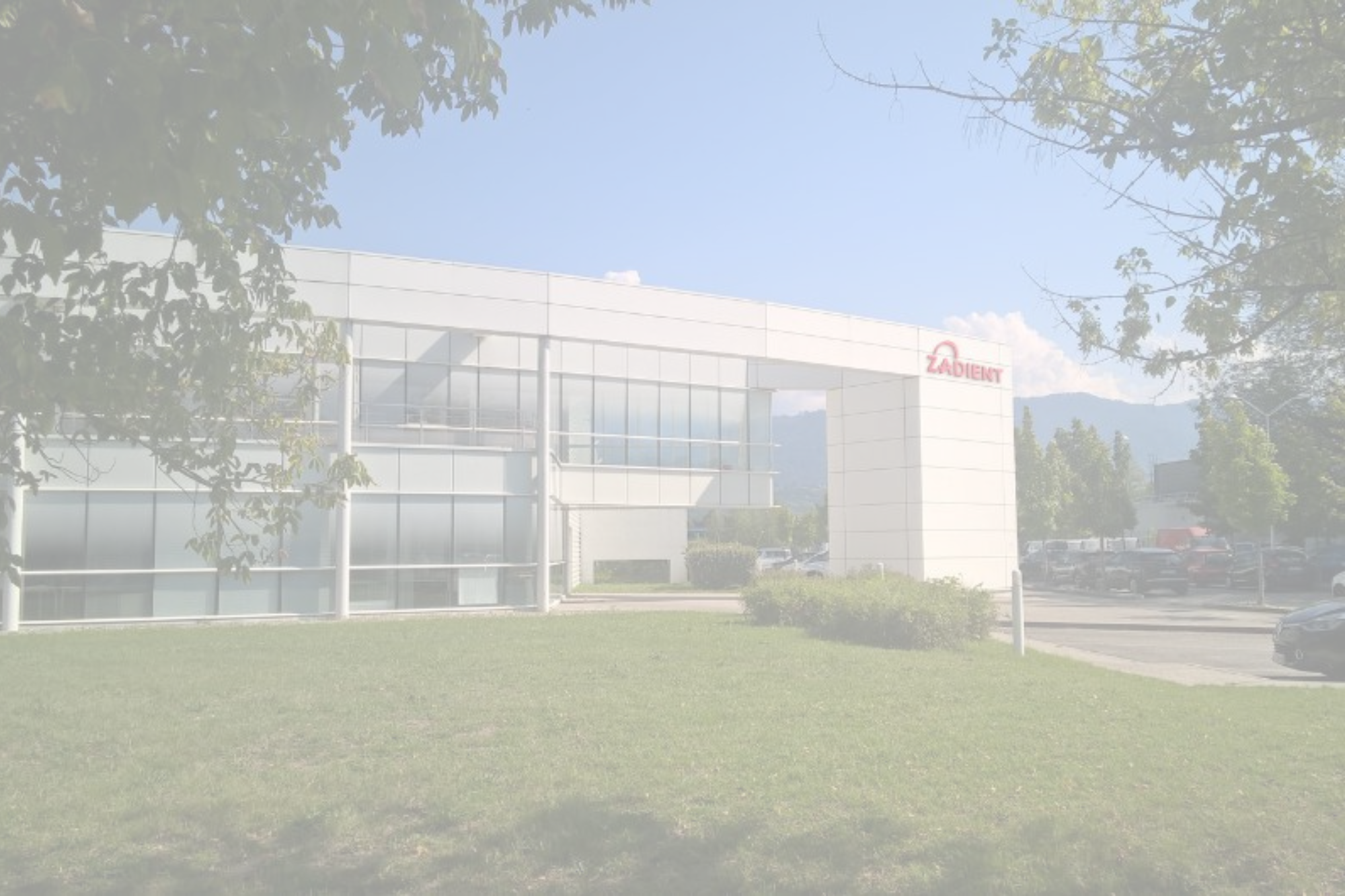
Zadient is headquartered in Chambery France between Geneva and Grenoble, at the heart of the French semiconductor ecosystem and the gateway to the Alps. Zadient conducts research in large diameter crystal growth yield improvements with the granular SiC source material it manufactures at its facility in Leipzig, Germany.

Chambery, France
Leipzig, Germany
Management
Zadient’s management team combines over 120 years of experience in fields such as chemical engineering, physics, and finance.

Kagan Ceran
CEO / Founder

Luc Hautemanière
CFO

Jan Richter
CQO

Hilmar Tiefel
COO CVD Technology

Friedrich Schaaff
CTO CVD Technology

Géraldine Pages
Human Resources VP
Board
Zadient’s board draws on the experience of its four main investors who among them have invested in and supported the development of over 75 portfolio companies.

Rudolf Staudigl
Chairman

Søren Hein
MIG Capital

İlker Temuzkuşu
Zorlu Capital

Wolfram Drescher
Blue Wonder Ventures

Klemens Brunner
Group Executive VP

Philippe Vercherin
Crédit Mutuel Impact

Zeina Chebli
European Innovation Council Fund
ESG
By the very nature of its business, Zadient is fully committed to protecting the environment and reducing CO₂ emissions. SiC semiconductor devices improve energy efficiency compared to Si devices and Zadient’s SiC materials go even further to improve the efficiency with which these SiC devices are produced themselves.
Leading experts have calculated that SiC devices remove 13 times more CO₂ from the atmosphere during their operating lifetimes than is emitted during their production relative to Si devices.* Regardless, Zadient works every day to improve the energy efficiency of its production processes and reduce their footprint.
Zadient is also committed to diversity, equity and inclusion in all of its social relationships, including with its employees, customers, suppliers, contractors, and community.
Zadient practices the highest standards of corporate governance, with leading firms as its external accountants and auditors.
*BPEI/Wolfspeed, 2021


